Direct Links
Tuesday, March 30, 2010
ISP Flash Microcontroller Programmer
Hardware
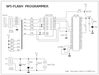
Figure 1 shows the circuit diagram of the in-system programmer interface, the power to the interface is provided by the target system. The 74HCT541 ic isolate and buffer the parallel port signals. It is necessary to use the HCT type ic in order to make sure the programmer should also work with 3V type parallel port.
More information (PCB, descriptions, Programmer software can be found at the following Link)
Link to main site
Subscribe to Electronics Circuits by Email
Monday, January 11, 2010
Single chip(MAX 2606) based FM transmitter circuit
Here’s a single chip FM transmitter circuit using Maxim semiconductors IC MAX2606. The MAX2606 is a compact, high-performance intermediate frequency VCO specially designed for wireless communication circuits. They have monolithic construction with low-noise and a low-power operation in a compact 6-pin SOT23 packing .Th1s low-noise IC feature an on-chip varicap diode and feedback capacitances that avoid the need for external tuning components, making the MAX2606 perfect for portable systems. Only an external inductor is needed to set the oscillation frequency.In addition to this, an
integrated differential output buffer is also there for driving a mixer or prescaler.The MAX2606 can be operated from a single +2.8 V to +5.4V supply and consumes very less current .The chip can be operated from 45MHz to 650MHz .
In the circuit the nominal frequency is set to 100 Mhz by inductor L1, (390nH) . The left and right channel audio signals from your source are added by R3 and R4, and attenuated by the POT R2. R2 can be used as a volume control .POT R1 can be used to select a channel of transmission between 88Mhz and 108Mhz.Use 80 cm long wire as the antenna .
- Assemble the circuit on a good quality PCB or common board.
- Use a battery for powering the circuit.It will reduce noise.
- An FM antenna from a old radio is a better option than the wire antenna.
IC1 is a voltage-controlled oscillator with integrated varactor. Its nominal frequency of oscillation is set by inductor L1, and a 390nH value places that frequency at 100MHz. Potentiometer R1 then lets you select a channel by tuning over the FM band of 88MHz to 108MHz. Output power is about -21dBm into 50 (most countries accept emissions below 10dBm in the FM band).
The audio unit's left and right audio signals are summed by R3 and R4, and attenuated by the (optional) potentiometer R2. R2's wiper signal serves as a volume control by modulating the RF frequency. Signals above 60mV introduce distortion, so the pot attenuates down from that level.
In the absence of a standard FM radio antenna, 75cm (30 inches) of wire will suffice as a transmitting antenna. For best reception, it should be mounted parallel with the receiving antenna. The IC operates on a single supply voltage in the range 3V to 5V, but one must regulate the applied voltage to minimize frequency drift and noise.
Thursday, December 31, 2009
Radio Remote Control using DTMF
The remote control transmitter consists of DTMF generator and an FM transmitter circuit. For generating the DTMF frequencies, a dedicated IC UM91214B (which is used as a dialer IC in telephone instruments) is used here. This IC requires 3 volts for its operation. This is provided by a simple zener diode voltage regulator which converts 9 volts into 3 volts for use by this IC. For its time base, it requires a quartz crystal of 3.58 MHz which is easily available from electronic component shops. Pins 1 and 2 are used as chip select and DTMF mode select pins respectively. When the row and column pins (12 and 15) are shorted to each other, DTMF tones corresponding to digit 1 are output from its pin 7. Similarly, pins 13, 16 and 17 are additionally required to dial digits 2, 4 and 8. Rest of the pins of this IC may be left as they are. The output of IC1 is given to the input of this transmitter circuit which effectively frequency modulates the carrier and transmits it in the air. The carrier frequency is determined by coil L1 and trimmer capacitor VC1 (which may be adjusted for around 100MHz operation). An antenna of 10 to 15 cms (4 to 6 inches) length will be sufficient to provide adequate range. The antenna is also necessary because the transmitter unit has to be housed in a metallic cabinet to protect the frequency drift caused due to stray EM fields. Four key switches (DPST push-to-on spring loaded) are required to transmit the desired DTMF tones. The switches when pressed generate the specific tone pairs as well as provide power to the transmitter circuit simultaneously. This way when the transmitter unit is not in use it consumes no power at all and the battery lasts much longer.
The receiver unit consists of an FM receiver (these days simple and inexpensive FM kits are readily available in the market which work exceptionally well), a DTMF-to-BCD converter and a flip-flop toggling latch section. The frequency modulated DTMF signals are received by the FM receiver and the output (DTMF tones) are fed to the dedicated IC KT3170 which is a DTMF-to-BCD converter. This IC when fed with the DTMF tones gives corresponding BCD output; for example, when digit 1 is pressed, the output is 0001 and when digit 4 is pressed the output is 0100. This IC also requires a 3.58MHz crystal for its operation. The tone input is connected to its pin 2 and the BCD outputs are taken from pins 11 to 14 respectively. These outputs are fed to 4 individual ?D? flip-flop latches which have been converted into toggle flip-flops built around two CD4013B ICs. Whenever a digit is pressed, the receiver decodes it and gives a clock pulse which is used to toggle the corresponding flip-flop to the alternate state. The flip-flop output is used to drive a relay which in turn can latch or unlatch any electrical appliance. We can upgrade the circuit to control as many as 12 channels since IC UM91214B can generates 12 DTMF tones. For this purpose some modification has to be done in receiver unit and also in between IC2 and toggle flip-flop section in the receiver. A 4-to-16 lines demultiplexer (IC 74154) has to be used and the number of toggle flip-flops have also to be increased to 12 from the existing 4
Download PCB (EXPRESS PCB FORMAT)
1) Transmitter Section - download-it
2) Receiver Section - download-it
3) Front panel (for cabin) - download-it
4) Data flow Diagram (PPT) - download-it
Subscribe to Electronics Circuits by Email
Monday, November 30, 2009
MAINS operate Christmas Star
Here is a low-cost circuit of Christmas star that can be easily constructed even by a novice. The main advantage of this circuit is that it doesn’t require any step-down transformer or ICs. Components like resistors R1 and R2.capacitors C1, C2, and C3, diodes D1 and D2, and zener ZD1 are used to develop a fairly steady 5V DC supply voltage that provides the required current to operate the multivibrator circuit and trigger triac BT136 via LED1.
LED Lighting For Christmas
Using light effects for decoration on festive occasions is a normal practice. Designers are coming up with varieties of electronic circuits to fill the imagination of users. Here is an easy-to-assemble circuit for christmas decoration as shown in Fig.1. It comprises four transistors, eighteen LEDs, a few resistors and two capacitors. Transistors T1 and T2 are configured as an astable multivibrator, which means one of the two transistors is always conducting. Thus the combination produces clock pulses. The values of time-constants formed with R6-C2 and R8-C1 pairs have been selected to produce a lowfrequency clock that is visible to human eye. The collectors of transistors T1 and T2 are connected to driver transistors T3 and T4. These are used to light up two rows of LEDs connected in parallel with alternate clock pulses. The frequency at which LED1 through LED9, and LED10 through LED18, alternately light up is about 2 Hz. You can easily change this frequency by changing the values of capacitors C2 and C1.
The middle one is the positive supply, which goes to the anodes of all LEDs. The outer track is connected to the cathodes of the red LEDs and the inner tracks are connected to the cathodes of the green LEDs.
To obtain the best effect with the combination of red and green LEDs, mount them alternately on the PCB board. Exercise care so that you do not accidentally connect the red and green LEDs in parallel. The forward voltage drops of red and green LEDs are different. The circuit works off a 3V-9V battery. It consumes little current, so two/ four AA cells or a 9V battery can easily power the electronic star. You can also use a stabilised 3V-9V DC mains adap-
Fig.1: LED lighting circuit for Christmas tor in place of the battery.
Reference : EFY
www.electronicsforu.com/electronicsforu/lab/ad.asp?url=/EFYLinux/circuit/December2007/CI-01_Dec07.pdf&title=LED%20Lighting%20for%20Christmas