Custom Search

Monday, January 30, 2012

Monday, January 31, 2011

Thursday, October 28, 2010

Thursday, September 23, 2010

20W audio amplifier using LM1875

Subscribe to Electronics Circuits by Email

This is just another 20W audio amplifier circuit , but this time based on the LM1875 audio amplifier IC from National Semiconductors. With a 25V dual power supply LM1875 can deliver 20W of audio power into a 4 ohm speaker. The LM1875 requires very less external components and has very low distortion. The IC is also packed with a lot good features like fast slew rate, wide supply voltage range, high output current, high output voltage swing, thermal protection etc. The IC is available in TO-220 plastic power package and is well suitable for a variety of applications like audio systems, servo amplifiers, home theatre systems etc.
Read more: http://www.circuitstoday.com/20w-audio-amplifier-using-lm1875#ixzz11VTC9Fzh
Under Creative Commons License: Attribution

Wednesday, June 30, 2010

All about Solar Panels

Subscribe to Electronics Circuits by Email


I hope to cover this article with the following. Don’t know I have succeed in this.

What are solar panels?
How do solar panels work?
How to make panels?

Solar Panels use arrays of solar photovoltaic cells to convert incoming photons from sun into usable electricity. With solar panels we are using echo friendly renewable energy from the sun.

Solar panels are typically constructed with crystalline silicon, and the more expensive gallium arsenide, which is produced exclusively for use in photovoltaic (solar) cells.

Other, more efficient solar panels are assembled by depositing amorphous silicon alloy in a continuous roll-to-roll process. The solar cells created from this process are called Amorphous Silicon Solar Cells, or A-si. Solar Panels constructed using amorphous silicon technology is more durable, efficient, and thinner than their crystalline counterparts.

For very important solar projects, such as space probes, very-high efficiency solar cells are constructed from gallium arsenide by a process called molecular beam epitaxy. Solar cells constructed by this process have several p-n junction diodes, each designed to be maximally efficient at absorbing a given part of the solar spectrum. These solar panels are much more efficient than conventional types, but the process and materials involved make them far too expensive for everyday applications.

Solar panels collect solar radiation from the sun and actively convert that energy to electricity. Solar panels are comprised of several individual solar cells. These solar cells function similarly to large semiconductors and utilize a large-area p-n junction diode. When the solar cells are exposed to sunlight, the p-n junction diodes convert the energy from sunlight into usable electrical energy. The energy generated from photons striking the surface of the solar panel allows electrons to be knocked out of their orbits and released, and electric fields in the solar cells pull these free electrons in a directional current, from which metal contacts in the solar cell can generate electricity. The more solar cells in a solar panel and the higher the quality of the solar cells, the more total electrical output the solar panel can produce. The conversion of sunlight to usable electrical energy has been dubbed the Photovoltaic Effect. The photovoltaic effect arises from the properties of the p-n junction diode; as such there are no moving parts in a solar panel.

Monday, May 31, 2010

Lead-acid storage battery

History of Lead Acid Battery


The lead-acid storage battery, an important energy storage device, is the most widely used secondary storage cell by automobile and other industries. Storage cells are devices which release a flow of electron through an external circuit as a result of reactions occurring between the active electrode materials and ions transported by the electrolyte. The cells in which the reactions are reversible are called secondary cells. In these cells the active materials can be returned to their original state by applying electrical current from an external source in the opposite direction to the flow of the cells discharge current.

In the early nineteenth century, scientists discovered that when direct current was passed between some pairs of electrodes of the same metal immersed in an electrolyte, the electrodes became polarized, i.e. when the circuit was opened a difference of potential existed between the electrodes. If they were connector, together a current flowed. Based on these experiments, in 1959
Gasten Plant began to investigate such cell using two electrodes immersed in dilute sulfuric acid. He found that appreciable currents could be obtained from the cell, after it was charged to produce a coating of lead peroxide on the positive plate. This was a major breakthrough in the field of electro chemistry.
Since then major developments have taken place in basic material of construction of lead-acid batteries. The present construction of this type of battery consists of positive electrode made up of leap peroxide, negative electrodes of lead in highly active metallic sponge. The insulating layers are made of hard rubber, PVC etc. The electrolyte is a dilute aqueous solution of sulphuric acid and container is marie of plastic, glass, rubber or polypropylene.

In 1940's six volt rubber case, featuring external cell connectors were available. Ford company offered codar separators and thirteen percent (13%) antimony grid alloys. The battery had a temperature compensating,vibrating contact voltage regulator. By the end of the 50's twelve volt battery was available featuring rubber separators and seven percent antimony in the grid alloy.
Towards the end of the 60's, the typical new car battery featured, through partition connectors, one piece cover, and sealed side terminals, a rubber container and grid alloy containing four percent antimony. Some of the leading battery manufacturers also introduced polypropylene containers at that time.

During the latter half of 70's the battery industry entered the maintenance free era. Grids with 1-2% antimony and other alloya like Ca, sn and plates made by high speed continuous strip processing equipment were introduced. In place of conventional separators plates, encapsulated in plastic envelopes came as new technology. The polypropylene container became a cocoon, completely sealing the battery against entry and containing subsystems, such as build-in state of charge indicators, and flame arresting vent system. In early 80's major changes tookplace in the technology of manufacturing systems, like continuous automatically controlled casting, rolling,grid expansion, pasting, curing cutting and stacking of battery plates.. This enhanced the roduction rates to a level undreamed of ten years earlier. In the modern plants up above the plate line, active material ingredients are programmed, weighed, and blended by computer controlled paste mixers, resulting in control of plate weight, thickness and chemistry, which was not possible few years ago. Control of this production system is backed up by analytical equipment, such as the atomic absorption spectrograph, florescent xray spectrometers, particle distribution counter and optical emission spectrograph. Sophisticated welding machines are common in all battery plants in USA, UK, Canada and France.

At present a great deal of emphasis is on the need of smaller and lighter batteries, for new small sized car and automobiles. The drive for improved fuel economy and the space limitations of present and planned engine compartments, are still strong factors today for the development of small, light weight, high powered batteries.

Chemical Reaction
Batteries use a chemical reaction to do work on charge and produce a voltage between their output terminals.

The reaction of lead and lead oxide with the sulfuric acid electrolyte produces a voltage. The supplying of energy to and external resistance discharges the battery.
The discharge reaction can be reversed by applying a voltage from a charging source.
Subscribe to Electronics Circuits by Email
Tuesday, March 30, 2010

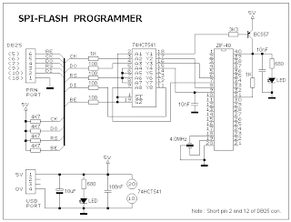
ISP Flash Microcontroller Programmer

Introduction

This ISP Programmer can be used either for in-system programming or as a stand-alone spi programmer for Atmel ISP programmable devices. The programming interface is compatible to STK200 ISP programmer hardware so the users of STK200 can also use the software which can program both the 8051 and AVR series devices.

Hardware

Figure 1 shows the circuit diagram of the in-system programmer interface, the power to the interface is provided by the target system. The 74HCT541 ic isolate and buffer the parallel port signals. It is necessary to use the HCT type ic in order to make sure the programmer should also work with 3V type parallel port.


More information (PCB, descriptions, Programmer software can be found at the following Link)
Link to main site

Subscribe to Electronics Circuits by Email

Monday, January 11, 2010

Single chip(MAX 2606) based FM transmitter circuit

Here’s a single chip FM transmitter circuit using Maxim semiconductors IC MAX2606. The MAX2606 is a compact, high-performance intermediate frequency VCO specially designed for wireless communication circuits. They have monolithic construction with low-noise and a low-power operation in a compact 6-pin SOT23 packing .Th1s low-noise IC feature an on-chip varicap diode and feedback capacitances that avoid the need for external tuning components, making the MAX2606 perfect for portable systems. Only an external inductor is needed to set the oscillation frequency.In addition to this, an
integrated differential output buffer is also there for driving a mixer or prescaler.The MAX2606 can be operated from a single +2.8 V to +5.4V supply and consumes very less current .The chip can be operated from 45MHz to 650MHz .

In the circuit the nominal frequency is set to 100 Mhz by inductor L1, (390nH) . The left and right channel audio signals from your source are added by R3 and R4, and attenuated by the POT R2. R2 can be used as a volume control .POT R1 can be used to select a channel of transmission between 88Mhz and 108Mhz.Use 80 cm long wire as the antenna .


Thursday, December 31, 2009

Radio Remote Control using DTMF

Here is a circuit of a remote control unit which makes use of the radio frequency signals to control various electrical appliances. This remote control unit has 4 channels which can be easily extended to 12. This circuit differs from similar circuits in view of its simplicity and a totally different concept of generating the control signals. Usually remote control circuits make use of infrared light to transmit control signals. Their use is thus limited to a very confined area and line-of-sight. However, this circuit makes use of radio frequency to transmit the control signals and hence it can be used for control from almost anywhere in the house. Here we make use of DTMF (dual-tone multi frequency) signals (used in telephones to dial the digits) as the control codes. The DTMF tones are used for frequency modulation of the carrier. At the receiver unit, these frequency modulated signals are intercepted to obtain DTMF tones at the speaker terminals. This DTMF signal is connected to a DTMF-to-BCD converter whose BCD output is used to switch-on and switch-off various electrical appliances (4 in this case).

Updated Circuit

The remote control transmitter consists of DTMF generator and an FM transmitter circuit. For generating the DTMF frequencies, a dedicated IC UM91214B (which is used as a dialer IC in telephone instruments) is used here. This IC requires 3 volts for its operation. This is provided by a simple zener diode voltage regulator which converts 9 volts into 3 volts for use by this IC. For its time base, it requires a quartz crystal of 3.58 MHz which is easily available from electronic component shops. Pins 1 and 2 are used as chip select and DTMF mode select pins respectively. When the row and column pins (12 and 15) are shorted to each other, DTMF tones corresponding to digit 1 are output from its pin 7. Similarly, pins 13, 16 and 17 are additionally required to dial digits 2, 4 and 8. Rest of the pins of this IC may be left as they are. The output of IC1 is given to the input of this transmitter circuit which effectively frequency modulates the carrier and transmits it in the air. The carrier frequency is determined by coil L1 and trimmer capacitor VC1 (which may be adjusted for around 100MHz operation). An antenna of 10 to 15 cms (4 to 6 inches) length will be sufficient to provide adequate range. The antenna is also necessary because the transmitter unit has to be housed in a metallic cabinet to protect the frequency drift caused due to stray EM fields. Four key switches (DPST push-to-on spring loaded) are required to transmit the desired DTMF tones. The switches when pressed generate the specific tone pairs as well as provide power to the transmitter circuit simultaneously. This way when the transmitter unit is not in use it consumes no power at all and the battery lasts much longer. Updated Circuit -(Bug Free)

The receiver unit consists of an FM receiver (these days simple and inexpensive FM kits are readily available in the market which work exceptionally well), a DTMF-to-BCD converter and a flip-flop toggling latch section. The frequency modulated DTMF signals are received by the FM receiver and the output (DTMF tones) are fed to the dedicated IC KT3170 which is a DTMF-to-BCD converter. This IC when fed with the DTMF tones gives corresponding BCD output; for example, when digit 1 is pressed, the output is 0001 and when digit 4 is pressed the output is 0100. This IC also requires a 3.58MHz crystal for its operation. The tone input is connected to its pin 2 and the BCD outputs are taken from pins 11 to 14 respectively. These outputs are fed to 4 individual ?D? flip-flop latches which have been converted into toggle flip-flops built around two CD4013B ICs. Whenever a digit is pressed, the receiver decodes it and gives a clock pulse which is used to toggle the corresponding flip-flop to the alternate state. The flip-flop output is used to drive a relay which in turn can latch or unlatch any electrical appliance. We can upgrade the circuit to control as many as 12 channels since IC UM91214B can generates 12 DTMF tones. For this purpose some modification has to be done in receiver unit and also in between IC2 and toggle flip-flop section in the receiver. A 4-to-16 lines demultiplexer (IC 74154) has to be used and the number of toggle flip-flops have also to be increased to 12 from the existing 4

Download PCB (EXPRESS PCB FORMAT)

1) Transmitter Section - download-it
2) Receiver Section - download-it
3) Front panel (for cabin) - download-it

4) Data flow Diagram (PPT) - download-it

Subscribe to Electronics Circuits by Email

Monday, November 30, 2009

MAINS operate Christmas Star

Subscribe to Electronics Circuits by Email

Here is a low-cost circuit of Christmas star that can be easily constructed even by a novice. The main advantage of this circuit is that it doesn’t require any step-down transformer or ICs. Components like resistors R1 and R2.capacitors C1, C2, and C3, diodes D1 and D2, and zener ZD1 are used to develop a fairly steady 5V DC supply voltage that provides the required current to operate the multivibrator circuit and trigger triac BT136 via LED1.
The multivibrator circuit is constructed using two BC548 transistors (T1 and T2) and some passive components. The frequency of the multivibrator circuit is controlled by capacitors C4 and C5 and resistors R3 through R7. The output of the multivibrator circuit is connected to transistor T3, which, in turn, drives the triac via LED1. During positive half cycles of the multivibrator’s output, transistor T3 energizes triac BT136 and the lamp glows.

LED Lighting For Christmas

Subscribe to Electronics Circuits by Email

Using light effects for decoration on festive occasions is a normal practice. Designers are coming up with varieties of electronic circuits to fill the imagination of users. Here is an easy-to-assemble circuit for christmas decoration as shown in Fig.1. It comprises four transistors, eighteen LEDs, a few resistors and two capacitors. Transistors T1 and T2 are configured as an astable multivibrator, which means one of the two transistors is always conducting. Thus the combination produces clock pulses. The values of time-constants formed with R6-C2 and R8-C1 pairs have been selected to produce a lowfrequency clock that is visible to human eye. The collectors of transistors T1 and T2 are connected to driver transistors T3 and T4. These are used to light up two rows of LEDs connected in parallel with alternate clock pulses. The frequency at which LED1 through LED9, and LED10 through LED18, alternately light up is about 2 Hz. You can easily change this frequency by changing the values of capacitors C2 and C1.
Resistors R2 and R4 are used to set the current through the LEDs. Red (LED1 through LED9) and green LEDs (LED10 through LED18) are used for simulating christmas decoration effects. For the brightness variation, you can change the values of resitors R2 and R4. Take any general-purpose PCB and cut it into a star shape. Thereafter, assemble the circuit and solder the colour LEDs onto it such that it looks like a christmas star.
Alternatively, you can design the PCB in circular shape with a festive white lacquer finish on component side and conductor tracks on the other. Place the control circuit at the centre of the PCB board, with LEDs mounted along the outer edge as shown in Fig. 2. Along this edge, there are three circular tracks:
The middle one is the positive supply, which goes to the anodes of all LEDs. The outer track is connected to the cathodes of the red LEDs and the inner tracks are connected to the cathodes of the green LEDs.

To obtain the best effect with the combination of red and green LEDs, mount them alternately on the PCB board. Exercise care so that you do not accidentally connect the red and green LEDs in parallel. The forward voltage drops of red and green LEDs are different. The circuit works off a 3V-9V battery. It consumes little current, so two/ four AA cells or a 9V battery can easily power the electronic star. You can also use a stabilised 3V-9V DC mains adap-
Fig.1: LED lighting circuit for Christmas tor in place of the battery.

Reference : EFY
www.electronicsforu.com/electronicsforu/lab/ad.asp?url=/EFYLinux/circuit/December2007/CI-01_Dec07.pdf&title=LED%20Lighting%20for%20Christmas

Wednesday, October 28, 2009

Long Range FM Transmitter Circuit

Subscribe to Electronics Circuits by Email

This circuit is a circuit diagram fm transmitter. This circuit is somewhat different from the previous fm transmitter circuit. Transmitter circuit described here has the additional RF power amplifier stage, after the oscillator stage, to increase the power output of 200-250 milliwatts. With a good matching 50-ohm ground plane antenna or multi-element yagi antenna, this transmitter can provide a good enough signal strength to a distance of about 2 kilometers. The circuit built around transistor T1 (BF494) is the basic low-power variable-frequency VHF oscillator. A varicap diode circuit is included to change the frequency of the transmitter and to provide frequency modulation by audio signals. The output of the oscillator is about 50 milliwatts.
Transistor T2 (2N3866) forms a VHF-class power amplifier. This increases the oscillator signals’ power four to five times. Thus, 200-250 milliwatts of power produced at the collector of transistor T2. For better results, assemble the circuit on a good quality glass epoxy board and house the transmitter in the case of aluminum. Shield the oscillator stage using aluminum sheets. Transistor T2 must be mounted on the heat sink. Do not switch on the transmitter without a matching antenna. Adjust both trimmers (VC1 and VC2) for maximum transmission power. Adjust potentiometer VR1 to set the fundamental frequency near 100 MHz.

Coil winding details are given below:
L1 – 4 changes of 20 SWG wire close wound over 8mm diameter plastic former.
L2 – 2 changes of 24 SWG wire near top end of L1.
(Note: There is no core (ie air core) is used to coil on top)
L3 – 7 changed from 24 SWG wire close wound with 4mm diameter air core.
L4 – 7 changed from 24 SWG wire-wound on ferrite beads (choking)
Potentiometer VR1 is used to change the fundamental frequency whereas potentiometer VR2 is used as power control.

Simple DC to AC Inverter


This DC to AC inverter circuit work based on unstable multi vibrator does. In this circuit, IC CD4047 is chosen as a heart of unstable multi vibrator, because this IC type gives a complementary output that has opposite phase to another ( pin 10 and 11 as seen in Figure 1), and has 50 % duty cycle that satisfy to generate a pulse for inverter.

In order to increase the current out of multi
vibrator so enough to generate a higher AC power too, then we must use MOSFET IRFZ44. IRFZ44 gives out high current to drive a step-up transformer, so AC power is available at the high voltage side of transformer.
This circuit is called as simple DC to AC inverter because of the output haven't a sinusoidal signal

yet, so there are many harmonic signal at the output. To suppress this signal we must use a filter such as a capacitor C. Because of this simplicity this circuit is suitable only for lighting demand. To build a sinusoidal DC to AC inverter, we can use a PWM signal for driving a step-up transformer, such as at page of DC to AC inverter using AT89C2051.

Friday, October 23, 2009

Parrot Sounding AC door Bell

Here is a mains-operated doorbell that produces parrot-likesweet voice without requiring any musical IC. The circuit is cheap and easy to construct. The AC mains is fed to the circuit without using any step-down transformer.


The complete circuit is shown in Fig. 1. The main components of the circuit are a resistor-capacitor network, transistor BC337 and audio output transformer X1. The oscillation frequency depends on the combination of resistors R4 and R5 and capacitors C3, C4 and C5. When switch S1 is closed, the audio signal generated due to oscillations is amplified by transistor BC337 and parrot-like sound is reproduced from loudspeaker LS1 connected across the secondary of transformer X1. Here we have used an 8-ohm, 0.5W loudspeaker. The audio output transformer (X1) is normally used in transistor radio. The function of the audio output transformer is to transform the high impedance of the output amplifier to match the much lower impedance of the speaker. This is necessary to get an efficient transfer of the audio signal to the speaker. If a wrong audio transformer is used, the result can be low output and loss of tone quality.

The audio frequency tone across the speaker terminal is about 3 kHz. The dimensions of the audio transformer used in the experimental setup are shown in Fig. 2. The circuit is powered directly from 220V AC mains. The operating DC voltage obtained at the cathode of diode D1 is about 6V. However, if you press switch S1 continuously for a few seconds, the maximum voltage developed at this point may go up to 20 volts, which must be avoided to prolong the life of the circuit. R1 limits surge current in the circuit. The parallel combination of resistor R1 and capacitor C1 limits the circuit current to a safe level for circuit operation. R2 across C1 provides DC path for the current as well as a discharge path when the circuit is switched off. This is to prevent a possible shock to the operator by charged capacitor C1.

Subscribe to Electronics Circuits by Email

Tuesday, September 29, 2009

20 Watts RMS Amplifier Using TDA2004

Subscribe to Electronics Circuits by Email

The Circuit present here is a 20Watts Car Stereo Amplifier. The main features of this powerful MULTIWATT® package (a trademark of SGS-THOMSON Microelectronics), a power amplifier IC chips designed specifically for car radio application, are the high current capability (3.5A) and the capability to drive a very low impedance (down to 1.6R). Here is the schematic diagram of the standard circuit as shown in its data sheet.

Technical Specification of TDA2004

The TDA2004A is a class B dual audio power amplifier in MULTIWATT[ package specifically designed for car radio applications

ABSOLUTE MAXIMUM RATINGS

VS Opearting Supply Voltage 18 V
VS DC Supply Voltage 28 V
VS Peak Supply Voltage (for 50ms) 40 V
IO (*) Output Peak Current (non repetitive t = 0.1ms) 4.5 A
IO (*) Output Peak Current (repetitive f . 10Hz) 3.5 A
Ptot Power Dissipation at Tcase = 60°C 30 W
Tj, Tstg Storage and Junction Temperature –40 to 150 °C

(*) The max. output current is internally limited.

http://www.datasheetcatalog.org/datasheets/166/378181_DS.pdf


TDA2004 has low noise, low distortion, and robust. The robustness is supported by its operation safety protection features: very inductive loads, load dump voltage surge, overheating, output AC-ground short, fortuitous open ground. Other important things is space and cost saving : very low external components counts, and very simple mounting system with no need for electrical isolation between the package and the heat sink because the heat contact metal of the package is already connected to ground. [The above circuit's schematic diagram is taken from: SGS-THOMSON Microelectronic Data Sheet]
Subscribe to Electronics Circuits by Email

Wednesday, September 16, 2009

Strobe Light

Strobe lights are widely used by disco lovers to create wonderful visual effects in disco halls and auditoriam. The circuit of a battery operated portable miniature strobe light, which can be constructed using readily available inexpensive components, is described here. For convenience and simplicity, an ordinary neon lamp is used here in place of the conventional Xenon tube. The whole gadget can thus be easily accommodated in a small cabinet, such as a mains adaptor cover, with a suitable reflector for neon lamp to give a proper look. Since current requirement of this circuit is very small, it may be powered by two medium-size dry cells (3V) or Ni-Cd cells (2.4V). Transistors T1 and T2 in the circuit form a complimentary-pair amplifier. When switch S1 is momentarily depressed, the circuit oscillates because of the positive feedback provided via resistor R2 and capacitor C1 to the base of transistor T1. The sharp pulses in the secondary winding induce a high voltage in primary winding of transformer X1, which in fact is a line driver transformer (used in reverse) which is generally used in 36cm TV sets. High voltage pulses induced in primary side are rectified by diode D1 and rapidly charge reservoir capacitor C2 to nearly 300V DC. When switch S1 is released, capacitor C2 holds the voltage level for a finite period while capacitor C3 charges slowly through resistor R3. When voltage across capacitor C3 becomes high enough, neon strikes and the capacitor rapidly discharges through the lamp. When voltage across capacitor C3 falls below the extinguishing potential of neon lamp, it goes off and capacitor C3 starts charging again. This cycle keeps on repeating for a short time, based on the reservoir capacitor C2’s value. Precautions. The neon lamp flasher section of this circuit carries dangerously high voltages. All precautions should therefore be taken for protection. Before any repair work, discharge capacitor C2 using a short length of wire with a 100k resistor connected in series.

read More
http://www.electro-tech-online.com/electronic-projects/39-project-strobe-light.html

Monday, August 31, 2009

SG3525 DC Converter 12V to +35V,-35V

The selected switching topology is called a "push-pull" converter, because the transformer has a double primary (or a "centre-tapped" one, if your prefer). The centre tap is permanently connected to the car battery (via an LC filter to avoid creating peaks in the battery lines, which could affect other electronic equipment in the car). The two ends of the primary are connected to a pair of paralleled MOSFETs each that tie them to ground in each conduction cycle (Vgs of the corresponding MOSFET high).

These MOSFETs should be fast, able to withstand high currents (in excess of 30A each if possible) and have the lowest possible Rds(on). The proposed On-Semiconductor�s MTP75N06 can withstand 75Amp and has a Rds(on) below 10 milliohm. This is important, because the lower this resistance is, the less power they are going to dissipate when switching with a square waveform. Another alternatives are MTP60N06, or the more popular BUZ11 and IRF540.

Although the schematics show a previous bipolar push-pull stage, you can also connect the gate resistor directly to the output of the controlling IC, leaving out the transistors, as the SG3525 is capable to drive up to 500 mA (theoretically), more than enough to switch the MOSFETs fast.


Read More
http://sound.westhost.com/project89.htm

Thursday, July 30, 2009

Analog Audio Delay Line(3d Sound)

It is fun to make a variable space in your small room, but it’s hard to make the actuator to move your wall or room partition. Using analog audio line delay, you can adjust your room virtually. Just turn a knob in your audio set and you can adjust your room size. The circuit described here will make your dream come true, giving a feel that your speaker is located 15 meters behind you, even though your room is actually 3 meters wide. Here is the circuit’s schematic diagram.The core of this circuit is SAD512D integrated circuit, an analog audio delay. The chip uses 512 capacitors memory to hold 512 sampled analog signal. The delay can be adjusted from about 5,1 ms to 51 ms by R12 pot. Feed the input of this analog delay circuit with a mixed right and left audio signals from your stereo system. The output of this circuit then fed to a small power amplifier and place the output speaker behind you. Now you can perceive like your speaker is 15 m away behind (with maximum delay setting). If you build two unit the cascading the circuit will result in 30 meter expansion of your virtual room.

The circuit consist three main block. The first block (U1A, U1B) is a fourth order low pass filter (-24dB roll-off per octave) with 2.5kHz cut off frequency. The second block is the adjustable analog delay integrated circuit (IC SAD512D). The delay is controlled by the oscillator around U2 which is adjustable from 5KHz to 50Khz. The last block is similar to the first block, a low-pass filter with 2.5KHz cut off frequency.

A variable resistor R9 is provided to adjust the input offset, avoiding signal clipping and maximizing the audio range. For easy adjustment, feed the input with high level audio signal until the output is distorted, then adjust R9 until the distortion is minimum, or if an oscilloscope is available, adjust the R9 until the clipping is equal for both positive and negative cycle. Finally, adjust R28 to give minimum sampling clock noise.

PARTS LIST

Reference Part
C1,C4,C10,C12 10n
C11,C2 1n5
C3 4.7uF/50V
C13,C5 1n9
C6 390p
C8,C7 1u/25V
C9 1uF/25V
C14,C15,C16 100n
J1 input connector
J2 out connector
R1,R2,R3,R5,R6,R7,R11,R20,R21,R22,R24,R25,R26 10k
R4,R23,R27 4k7
R8,R15 15k
R9 2k2 POT
R10 2k7
R12 220k POT
R13 10R
R18,R14 1k
R17,R16 330R
R19 100k
R28 250R trimpot
U1 TL084
U2 4011

Thursday, July 2, 2009

Temperature Monitor

Using a thermistor in the position shown makes a heat activated sensor. A change in temperature will alter the output of the op amp and energize the relay and light the LED. Swapping the position of the thermistor and 47k resistor makes a cold or frost alarm.

Sound Operated Switch

This sensitive sound operated switch can be used with a dynamic microphone insert as above, or be used with an electric (ECM) microphone. If an ECM is used then R1 (shown dotted) will need to be included. A suitable value would be between 2.2k and 10kohms. The two BC109C transistors form an audio preamp, the gain of which is controlled by the 10k preset. The output is further amplified by a BC182B transistor. To prevent instability the preamp is decoupled with a 100u capacitor and 1k resistor. The audio voltage at the collector of the BC182B is rectified by the two 1N4148 diodes and 4.7u capacitor. This dc voltage will directly drive the BC212B transistor and operate the relay and LED. It should be noted that this circuit does not "latch". The relay and LED operate momentarily in response to audio peaks.