Custom Search

Saturday, May 24, 2008

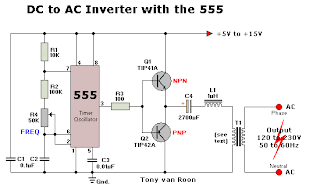
555 DC-AC Inverter

Parts List:
R1 = 10K
R2 = 100K
R3 = 100 ohm
R4 = 50K potmeter, Linear
C1,C2 = 0.1uF
C3 = 0.01uF
C4 = 2700uF
Q1 = TIP41A, NPN, or equivalent
Q2 = TIP42A, PNP, or equivalent
L1 = 1uH
T1 = Filament transformer, your choice

This DC-to-AC inverter schematic produces an AC output at line frequency and voltage. The 555 is configured as a low-frequency oscillator, tunable over the frequency range of 50 to 60 Hz by Frequency potentiometer R4.
The 555 feeds its output (amplified by Q1 and Q2) to the input of transformer T1, a reverse-connected filament transformer with the necessary step-up turns ratio. Capacitor C4 and coil L1 filter the input to T1, assuring that it is effectively a sine wave. Adjust the value of T1 to your voltage.

The output (in watts) is up to you by selecting different components.

Input voltage is anywhere from +5V to +15Volt DC, adjust the 2700uF cap's working voltage accordingly. Replacement types for Q1 are: TIP41B, TIP41C, NTE196, ECG196, etc. Replacement types for Q2 are: TIP42B, TIP42C, NTE197, ECG197, etc. Don't be afraid to use another type of similar specs, it's only a transistor... ;-)

TDA2030 typical application circuit

Friday, May 23, 2008

TDA2030 amplifier circuit to a single power law

Rated at 14 W. Power supply ± 6 ~ ± 18V. Output current, harmonic distortion and pay the small distortion (± 14V / 4 ohm, THD = 0.5%).

TDA2030 amplifier circuit to double the power law


Rated at 14 W. Power supply ± 6 ~ ± 18V. Output current, harmonic distortion and pay the small distortion (± 14V / 4 ohm, THD = 0.5%).

Ta7378P FM wireless microphone circuit

TA7378P using FM radio integrated block the production of FM wireless microphone, external components small, simple and easy system, work stability, particularly suitable for the production of radio enthusiasts. Figure FM wireless microphone for the specific circuit, ICl (TA7378P) includes RF amplifiers, mixers, to enlarge the buffer, the local oscillator circuit and bias, the regulator circuit.
The circuit Qiaomiaodejiang combination of internal circuits, use of the circuit-and AFC (automatic frequency control) the use of a variable capacitor oscillator circuit to generate FM (FM) waves.
In order to reduce the impact of external, in the oscillation between the mixer and a buffer amplifier has. Finally, RF amplifiers zoom through launch FM radio antenna.

99.6MHZ J-power FM transmitter antenna


99.6MHZ J-Power FM transmitter antenna

99.6MHZ J-power FM transmitter antenna 99.6MHZ J-power FM transmitter antenna

10 mm diameter brass refrigeration production with a total length of 3.5 M 10 mm diameter brass refrigeration production with a total length of 3.5 M

15 W transmitter power amplifier 88-108MHZ

The power amplifier can be reactive 1-2 W ,88-108MHZ power FM transmitter As for the expansion of 10-15 W, a single C Larger and multi-level low pass filter components, has a high conversion efficiency and strong Yi-wave suppression.
Circuit see attached map shows, using high-power launch of C1972, its parameters are as follows: 175 MHZ, 4A, 25W, power gain ≥ 8.5 db, as shown by parameters, circuit work center frequency of about 98 MHZ, the importation of about 2 W of RF power , The rated output up to 15 W.
To maintain 88 ~ 108 MHZ with any frequency output reached rating, according to the level before the center frequency of some components to make suitable adjustments. May, when necessary, to reduce low-ball-series, to increase power output. The expansion of the power signals from three low-pass filter Yi-filtered high element of the transmitting antenna feed.
Components choice: In addition to electrolytic capacitor, the other tiles with high-frequency capacitors, C11, C12, C14 use high-frequency characteristics of a good, stable performance of adjustable capacitors, inductors Choke RFC1, RFC2 finished with inductors, must pay attention to the current RFC2 Carrying capacity, should use the coarse diameter Cores with the inductors.
L1-L6 available ø0.8mm the high-intensity enameled wire system, a diameter of about 5 MM, a few laps in the plans to "T" for the units indicated. Q1 ordinary Q9 socket, and supporting the use of plugs. Q2 used for 50 Ω RF output connectors, and then of resistance is smaller, more conducive to impedance matching.
Larger effective power more common for the launch of the C1972, of course, especially if you sufficient money to buy blocks C2538 contour of the gain, power will be even greater.

Debug circuit, be sure to pay attention, the power circuit, we must connect false load (I use 30 1 W, 1500 Ω high-precision metal film resistors made parallel), and there must be enough in the cooling devices, normal working hours Power Of not less than 2.5 A, the antenna impedance strictly equivalent to 50 Ω, can not be used Duanbang drawbars antenna, or a strong current of RF feedback circuit will create their own interference, most of RF energy to space and can not be convergence in the consumption of power, to overheating Damage must be launched for 50 Ω coax, tabled Reply to launch outdoor antenna.
Circuit the normal work of the key lies in whether the circuit debugging, the whole process had to very carefully.
Debugging, enter only the smaller the incentive power supply voltage drop to 9 V, using high-frequency voltage (can not use ordinary multimeter) monitoring false load at both ends of high-frequency voltage value, regulating C12, C14, L3, L4, L5, L6 So that the voltage range of 15-20 V around, and then adjust C11, L1 voltage to the largest.
And then gradually raise the voltage, each raising a voltage repeatedly adjusted C12, C14 and C11, L1 so that the maximum output voltage, noted that the input voltage and RF power simultaneously increasing incentives to ensure the accuracy of the results of debugging. Reach rating, 13.8 V supply voltage of about 2 A current work around, 50 Ω-load resistance at both ends voltage ≥ 40 V, RF power output of 15 W.

With the RF power amplifier with 50 Ω-wide umbrella to the vertical launch antenna (gain of about 2 dB), to ordinary FM radio test fired from the coverage of not less than 15 KM
VHF UHF TV modulator

Simple TV Modulator that working on VHF UHF Band, the oscillator generates frequency is modulated with the video signal and the modulated carrier wave thus generated is fed into the TV set's aerial input via a cable. Then all that remains to do is tune the VHF UHF TV set to the correct frequency.
The harmonics generator converts the oscillator signal into a sort of frequency spectrum containing all the multiples of 27 MHz up to about 1800 MHz. The TV modulator's output signal is made up of a large number of little peaks, each of which is a complete transmitter signal. At least one of these will always be in band I (VHF channels 2. . . 4), one in band III (VHF channels S. . .12) and many of them will be in bands IV and V (UHF channels 21.. .69).

TV Transmitter Band I and III

This TV transmitter working on VHF Band I and III, using negative sound modulation and PAL video modulation. This is suitable for countries using TV systems B and G, like Australia and Indonesia.
This circuit has not been tested at UHF frequencies. The modulated sound signal contains 5.5 -6MHz by tuning C5. Sound modulation is FM and is compatible with UK TV Transmitter System I sound. The transmitter however is working at VHF frequencies between 54 and 216MHz (band I and Band III) and therefore compatible only with countries using Pal System B and Pal System G.

88-108 MHz Preamplifier

This VHF amplifier working on Band 2 Radio Spectrum tuning approximately 88 - 108 Mhz

The Preamplifier circuit uses two 2N3819 FET's in cascade configuration. The lower FET operates in common source mode, while the upper FET, operates in common gate, realizing full high frequency gain. The bottom FET is tunable allowing a peak for a particular station.
Coil details follow:
L1 4 turns of 18swg air spaced with a 1cm diameter, the tap is one turn up from earth end...
L2 4 turns of 18swg air spaced with 1 cm diameter. The coupling coil is 1 turn interwound from the supply end. Enamel coated wire must be used.

Making Simple TV transmitter

(1) Soundless version, You are familiar with the most simplest FM transmitter" that I designed (left). Let's try to transform it into a TV transmitter. Just change the input from the audio to the video (video camera or VCR) and check the signal at your television set: in Europe, for instance, choose the channel 2 - 4 and turn the trimmer cap of the transmitter. You will find some images or might watch a clear image. This suggests that it will be not so difficult to build a TV transmitter.

(2) Advanced Version (AV) , When you succeed in this version to work, you may try the advanced version (pdf). ( http://www.translocal.jp/microtv/20070704tvtx_rtctk01.pdf )
In this version, stability and quality are improved. This can have even the audio too. However, in order to complete this, you have to use a proper frequency counter.

FM Transmitter With Transistor 2SC1815

Will have to introduce a system of simple and small FM transmitter. Not only does it meet the requirements of the launch distance, but also at the same time using microphone and voice input signal line, background voice. Modulation circuit surveillance has also joined the table first, so that they can better control and the proper use of transmitters, the following circuit diagram, read briefly, whether it's just like a radio station equipment as many functions. Yes, this small transmitter can help you easily set up an amateur FM radio stations! 500 M in the coverage around. Echocardiography the bar, act immediately!
Principle small FM transmitter circuit components and options:

Signal to the microphone after intake, the C1 coupling into the BG1 and external circuit voltage of the single negative feedback amplifier, the voltage signal amplification weak enough to enlarge the extent of U1A and the line to enter the input signal with a mixed U1B. Mixed signal modulation way to the R17 from BG2 FET and the surrounding circuit composed of common than LC finishes the test, the test than the LC oscillator are characterized by a general three-capacitance oscillator simple, but also with high efficiency and high stability. Waveform, and modulation bandwidth, as this amateur production of FM transmitters appears to be particularly important.

Finally BG3 cast by the post-amplifier to enlarge the field by launching antenna fired by general can listen to FM radio broadcast. Another component of the signal through the amplifier to enlarge U1C after the wave rectifier D2 SR DC drive microamps table, Near and surveillance signal modulation rate. Use the system for general should not exceed 85 per cent suitable. GM and other integrated circuits using LM324 four operational amplifier and form a single power reverse input, both of the input voltage is set at half the supply voltage. Table surveillance for the first u-200, BG1.BG3 choose 2SC1815. BG2 three DO2 FET, D2 varactor diode using a S2267. Antenna require the use of 1 / 4 wavelength, such as the use of the best pull rod antenna not less than one metre. Otherwise effect will be less than overstaying launch. Final say about, please do not interfere with normal radio!

FM transmitter With uPC1651

The circuit has been produced by Japan's NEC as a major upc1651 IC devices, the high gain circuit, work stability, thereby ensuring the microphone performance. Use of FM transmitter. Used it 40 - 50 cm soft drag line for antenna, the effective range of more than 30 launch M. L carefully spacing adjustment and fine-tuning capacitor, will launch frequency coverage for 88 - 108 Mhz. Map L enameled wire with diameter of 0.51 mm in diameter, 4 mm cylindrical Tuitai from around 5 laps

FM Stereo Encoder CD4066

Circuit schematics IC1-4069 in the Y1, Y2 formation of a 76 KHZ frequency of the oscillator, the Y3-Y6 isolation plastic, into IC2 dual JK flip-flop CD4027 composed of two components- frequency circuit, a symmetrical + / 38KHZ-19 KHZ and the square wave, + / -38 KHZ IC3 the square used to control analog switches CD4066, a stereo audio input signal after switching modulation used for the 19 KHZ frequency mixed signal to the transistor into FM 9014 after isolation Modulator.
Click to access the debug FM modulator and 5 V power supply, with a multimeter measured IC1CD4069 the legs and IC2 CP, Q, Q, the legs should be half the supply voltage, the oscillator has been start-up. If a digital frequency meter measured IC1 output frequency, frequency regulation RW1 to 75 KHZ + /-10HZ can. If not, can be transferred to the prospective radios, RW2 half-good, and then transferred RW1, the bright lights stereo radio, and no speakers in the temple frequency whistle sounds. From the input into the stereo audio signal (1.5 Vpp, output amplifier available), this will be able to receive stereo radio broadcasting.

Input signal can be obtained from the line, but at R7 should be changed. Finally, can be transferred R7 to the smallest high-frequency noise, in fact R6, R7 equivalent BA1404 in 13, 14 feet of external components, the Pilot mixed signal and composite signal circuits, and input to the amplifier, the circuit of is 9014, and BA1404 from 12 feet on the entry.

Macsot MR-700 High Quality wireless microphone

This is collected by the Macsot MR-700 wireless microphone system launch of the circuit for maintenance reference. High Quality Audio on receiver output.
Active components:
  • Microphone or Audio Preamplifier with IC MC4458
  • Dynamic Audio processed with one NE571 From Philips
  • Frequency Oscillator generated by one crystal 20.05 MHz and Varactor diode 2CB11A. No drift frequency is guaranted.
  • 9V DC power supply or battery.

FM Stereo Transmitter With MC145151

This fm stereo transmitter use pll chip MC145151 from Motorola and stereo encoder chips BA1404 with vco built in. MC145151 IC used is to overcome the single-frequency instability in the BA1404. Modulation of the emission control BB910 frequency. B571C kept in control procedures, the procedures required to prepare another.

Parts List and Schematic

Component Values of the fm stereo transmitter you can find out the schematic. Please download schematic for enlarged image

Amplifier section of this FM Stereo transmitter uses a single 2sc2053 transistor with power out about 250 mWatt.

300mW FM Transmitter 2SC2538

The FM transmitter using a varactor diode way radio, plus a Class C amplifier, RF output power of up to 300 mW more open to more than one kilometer distance communications. Select the components of this fm transmitter: Q1 with ≥ 100 mA, Ft ≥ 300 MHz, β ≥ 100 tubes available 3 DG82, 3DG122, 3DG130, 2G711; Q2 with 2SC2538, 2SC1970, etc..
It must be noted in the fm transmitter assembly that RF Baffles circle L8, L9, L10; C13, C14, C17, C18, C19, and so can not be omitted, otherwise it would cause unnecessary self-excited oscillation. L1, L5 need to tap extraction, data such as icons, not otherwise due to impedance matching, the output power of less than maximum. Such as a battery-powered, Q3 (Darlington tube), C15, R6 can be omitted.

Debugging steps :
1. In the output termination of testing circuit to regulate the C7, C9, C12 to the largest multimeter readings,
2. Remove test circuit connected to one meter in length pole antenna to pull to fine-tune C12 simple reading of the largest field will be completed debugging.

MC1374 TV RF Modulator

The MC1374 includes an FM audio modulator, sound carrier oscillator, RF oscillator, and RF dual input modulator. It is designed to generate a TV signal from audio and video inputs. This TV RF modulator based MC1374 IC from Motorola with wide dynamic range and low distortion audio make it particularly well suited for applications such as video tape recorders, video disc players, TV games and subscription decoders.
The IC features:

  • Single Supply, 5.0 V to 12 V
  • Channel 3 or 4 Operation
  • Variable Gain TV RF Modulator
  • Wide Dynamic Range
  • Low Inter modulation Distortion
  • Positive or Negative Sync
  • Low Audio Distortion
  • Few External Components
For more info about TV RF Modulator, please download
datasheet - http://www.ziddu.com/download.php?uid=a7OdlJWlbbCbluKnZqqhkZSoY6ucnJWo6
application note
http://www.ziddu.com/download.php?uid=bqqelZesaa2bnJSltayZlJyiZ62WlZep7

Audio Video RF Modulator With LM2889

The LM2889 is designed to interface audio video RF modulator signals to the antenna terminals of a TV receiver. It consists of a sound sub carrier oscillator and FM modulator, video clamp, and RF oscillators and modulators for two low-VHF channels.
Audio Video RF Modulator with LM2889 allows video information from VTRs, video disk systems, games, test equipment, or similar sources to be displayed on black and white or color TV receivers.
Features :
  • Pin for pin compatible with LM1889 RF section
  • Low distortion FM sound modulator (less than 1% THD)
  • Video clamp for AC-coupled video
  • Low sound oscillator harmonic levels
  • 10V to 16V supply operation
  • DC channel switching
  • Excellent oscillator stability
  • Low inter modulation products
For the detail about this audio video RF modulator, please follow this link for datasheet.
http://www.ziddu.com/download.php?uid=bKufnJynZa+emZqnsayZlJyiY62WlZur3
Application Note
http://www.ziddu.com/download.php?uid=a6yflJimZqqcluKnZKqhkZSoYaugnZqu4

TV RF Amplifier 5W With BLW98

This application circuit is a TV RF amplifier for driving small UHF TV transmitters, with gain is 7dB and can amplify a signal between 470-860 MHz. Drive input the circuit with 1 to 1,5 Watts signal. Better use double layer PCB with the second layer connected to earth.
Use a stabilized power supply 24 volts and at least 5 Amps. The transistor case is the SOT-122A and be careful because the transistor is very toxic for your health. Tuning of this tv rf amplifier can be achieved turning the two variable capacitors. Do not forget to use heat sink for both transistors, specially for the BLW98 and it would be better if you place a small fan as well.
For more details for constructing this tv rf amplifier, please download datasheet
( http://www.ziddu.com/download.php?uid=ZbCcnJamZq6ampenr6yZlJyiYa2Wl5Wn1 )

20 dB VHF RF Amplifier

This RF amplifier is to strengthen a small signal in the region of VHF or FM, or it is we lead a body, or a receptor. The preamplifier that to you we propose offers 20dB in all the region of VHF and it still can reach also their 500MHZ.


The amplifier is a circuit of high frequency RF with distinguishable materials. The amplifier as circuit strengthens the tendency of signal with concrete aid, depending on the frequency of signal. If the frequency of signal is included in the limits of spectrum of frequencies of amplifier, then it is strengthened, otherwise it is downgraded. Each amplifier of this category, accordingly with his designing, strengthens a concrete region of frequencies and obeys in same characteristics. The one that to you we present today concerns the regions of VHF where they exist and the corresponding television stations for channels 5 until 12. His circuit he is enough simple, so that it is made easily with materials that exist in the trade. It is based on transistors with aid until the 500MHZ. The type of transistor can be BF197 or some other.

It appears the theoretical circuit of amplifier. As we see it is constituted from two similar circuits (rungs). In this circuits are not included in joint action circuits. With that way is covered a wide spectrum of frequencies, without is differentiated abruptly the aid as for the frequency. With this provision we have smaller gain but big breadth of frequencies. The two rungs are same, with the same prices of materials and each rung offer aid roughly 10dB. The transistors and the remainder materials, because the industrial manufacture, have almost the same characteristics. Associates the particular characteristics of demagogues are altered mainly the aid of rung. Each rung uses a transistor of type npn in provision of common emitter that functions in order A. his rungs works in provision of common emitter with null resistance in emitter. In each rung a network of resistances between the collectors and the bases polarize the transistors and ensures the operation of circuit. The junction between the rungs becomes via ceramic capacitors of small capacity from 0,1nF until 0,22nF (at preference ceramic). In the place of two rungs we can try various transistors of independent company or even different between them. The circuit of course cannot work with all of them. The tendency of catering should emanate from stabilised power supply with tendency 12V. Depending on the tendency of catering and the type of transistor, in each rung of amplifier it needs enter also different resistances. Force of expense, under conditions of high excitation it can exceed the 1 mW.


500mW FM PLL Transmitter 88-108MHz

FM transmitters have always been fascinating and one can find thousand examples of them on the internet. Sadly most of them are full of error and miss leading information. Most of them also have low stability and frequency drift, many coils and components which are difficult to find. The output power is often set to several watts with just a transistor or two…..can't fool me. So therefore I decided to construct a simple transmitter with great performances.

Some contruction achievements I wanted were:
# Simple construction
# Commonly components
# High quality and stability
# Low number of coils
# High output power

The frequency of this transmitter can easy be changed with software and space/compress an air coil, simple don't you say? The basic hart of this transmitter is a colpitts oscillator. The oscillator is a VCO (voltage controlled oscillator) which is regulated by a PLL circuit and PIC micro controller. Don't get upset now…it is not that difficult after all. Let's check the schematic and I will explain the function.

Hardware and schematic
Click on the pic to see the large schematic. The main oscillator is based around the transistor T1. This oscillator is called Colpitts oscillator and it is voltage controlled to achieve FM (frequency modulation) and PLL control. T1 should be a HF transistor to work well, but in this case I have used a cheap and common BC817 transistor. The oscillator needs a LC tank to oscillate properly. In this case the LC tank consist of L1 with C1, C2, C3, and the varicap BB139. The coil is parallel with C1 and C2 which are in serial . The same with the varicap and C3. You can think that L is parallel with [ (C1//C2) + (Varicap//C3)] The value of C3 will set the VCO range. The large value of C3 the wider will the VCO range be. Since the capacitance of the varicap is dependent of the voltage over it, the capacitance will change with changed voltage. When the voltage change, so will the oscillating frequency. In this way you achieve a VCO function.

PLL and Microcontroller
The oscillator is made to work as "Voltage Controlled Oscillator" VCO.
To control the frequency a synthesizer circuit LMX 2306 has been added. The PLL circuit has a pickup coil (L2) connected to pin 6. This coil should be put close to the L1 coil for picking up some of the oscillating energy. The PLL in the LMX2306 will then use this frequency to regulate the VCO and lock it to desired frequency. The regulating system also need an external reference crystal. In this case I use 12.8 MHz.

At pin 2 of MX2306 you will find a PLL filter to form the Vout which is the regulating voltage of the VCO. The PLL try to regulate the Vout so the oscillator keeps the frequency locked to desired frequency. The desired frequency is programmed into the PIC EEPROM and is clocked into the synthesizer (LMX2306) at power up. I will below explain how to program the EEPROM for different frequencies. At pin14 of the synthesizer you have a control output. At this output you will find the reference frequency for testing. (I must warn you because the signal is not symetrical in shape. The positive pulse are only a few microsecond so you will have difficult to see it at oscilloscope.) I solved it by connecting it to a 74HC4020 (14-stage Binary Counter) to pin 10 Clock input. At Q0 (pin 9) you will have a symmetrical square wave with half frequency since the circuit is a counter. At Q1 pin 7 it will be divided by 4, see datasheets for more info.

LF input
The audio you wish to transmit should be connected to the Audio input (left side of schematic).
The signal will affect the varicap and thereby Frequency Modulate FM the RF carrier. A potentiometer P1 has been added to set the modulation depth (Wide FM or Narrow FM). You may have to play a bit with the value of P1 because it tends to modulate to much. You may have to add a 500k - 1M potentiometer instead. You test and find out yourself.

Buffer stage
Here you find another HF transistor and it is working in class C. The resistor R1 and the resistor Re2 set the DC current. In this case I found that 9.1k will give good output power and so the same with 150. If you wish to increase the power Re2 should be lower. You can add another 150 ohm resistor parallel.

In the table below I show you the output power with different voltages and values of resistor Re2. I advice you not to run this transmitter with to high output power. The transistor I use is a small one and tends to get hot. I advice you to run the unit from 0 - to 200mW. At 500mW the transistor will be in pain...*smiling* At the output you will find a T network. This "filter" will match the antenna impedance to the transmitter output stage. You have two variable capacitors 60pF to tune the transmitter for best performances.

The antenna I used I a 1/4 wave whip antenna (wire) about 75cm long. This type of antenna is smaller but not so good performance as a dipole. With a dipole you will be able to transmitter much longer distance.

How long can I transmit?
That is a very difficult question because the environment affect the transmitting distance very much. In a city environment with concrete buildings the transmitter will send maybe 200m.
I an open filed it will transmit 2000m. I did a filed test and with 70mW output power into the "bad" whip antenna placed indoors I could transmit 200-300m out into a park with no problem.

Output power
Table below show you the power measurements I have done. The Re2 is 150 ohm and in some test I connect a 50 ohm parallel. The output power in measured into a dummy load of 50 ohm.


Testing
The first thing you should test is that the oscillator is working. I disconnected the Vout from pin 2 of the PLL LMX2306. I then connected Vout to ground and check the oscillator. The oscillator should now oscillate at the lowest frequency. With my Wireless frequency counter I found that the oscillator was working at 100 MHz. I streatched the coil L1 a bit until it oscillated at 105 MHz. I then connected Vout to +5V and now the oscillator was oscillating at 108MHz. Great!, just as I wanted. By changing the Vout from 0 to +5V I could change the oscillating frequency from 105 to 108 MHz. I then reconnected the Vtune to the PLL.

Download PIC16F870 programs (INHX8M format)
The zip file contains several hex files made for different frequencies (88 to 108) MHz.
fm_500.zip( http://hem.passagen.se/communication/pic/fm_500.zip ) PLL software to FM transmitter (the hex files are zipped!).

Final word
This project is explaining how you can build a FM transmitter with great performances. I advice you not to use it because it is not legal. You can only use it with a dummy load, not with an antenna. If you choose to use an antenna I hope you will use it with good manner.

More Information --->( http://hem.passagen.se/communication/fm_500.html )

Phone FM Transmitter


This FM transmitter attaches in series to one of your phone lines. When there is a signal on the line (that is, when you pick up the handset) the circuit will transmit the conversation. In particular it will radiate from the phone line itself. It is a passive device - there is no battery. It uses the signal on the phone line for power. No aerial is needed - it feeds back the RF signal into the phone line which radiates it in the FM band.

The frequency of transmission may be adjusted by the trim cap. L1 is 6 turns of enameled wire, L2 is 8 turns and L3 is 6 turns. Spread out L3 coil about 1 mm apart. The coils should not touch. a solder connection (or tap) is required from the top of the first turn in the L3 coil to the pad next to the coil. Solder a piece of wire to the top of the first turn as shown on the overlay. Then solder the other end to the pad immediately next to the L3 coil. R1 & C4 act as a low pass filter. C3 is a high frequency shunt. L2 is a RFC (radio frequency shunt.) It decouples the power and audio from the transmitter amplifier circuit. L1 and C6 should be adjusted to match a frequency on your FM receiver. With C1 at 27p you will find that the kit tunes into the FM band in the 86 - 95 MHz area. With C1 at 22p the band is raised to about 90-95mhz (depending in the coil spacing.)

If you want to move this tunable area still higher to over 100MHz range then replace C1 by a 15pF or 10pF capacitor. You can experiment to get greater transmission range away from the phone line by adding an aerial (about 150 cm of 26 gauge wire) to the collector of T2.

Thursday, May 15, 2008

STK0060 60W


Features of STK0060:

General output stage of power amplifier has a difficult and complex problem about heat sink designing and its settings. Sanyo's DP intends to decrease electronic parts and rationalize a manufacturing process by designing IC of only output stage pf power amplifier.

  • IMST Systems
  • Output stage for AF high power amplifier.
  • Dual power supply
  • Darlington type pure/ quasi-complementary circuit
  • These same pin assignment and pin interval lead to standardize a printed board.
  • Metal substrate use IMST makes good thermal stability
  • Able to design freely previous section of power amplifier. This leads tone control designing.
Equivalent Circuit.

Application Circuit Found the Data Sheet (SANYO)
Application Notes:

Maximum Ratings at Ta=25 deg C
Maximum Supply Voltage VCCmax +- 55V
Tehrmal resistance 0j-c idealstage 1.3 deg C/W
Collector current Ic 8A
Juction Temperature Tj 150 Dec C
Storage Temperature Tstg -30 to +105 Deg C
Allowable Load Shorting Time ts VCC=+-41V, RL 1 Sec
=8 Ohm, Po=60W
f=50Hz

*Use an Appointed Transformer.

Recommented Operation Conditions at Ta=25 Deg C
Recommented Supply Voltage VCC +-41 V
Load Resitance RL 8 Ohm

Operation Characterestic at Ta=25 Deg C, VCC= +-39V, RL=8, Rg=600 Ohm
VG-36.7db at the appointed test circuit.

Min Typ Max unit
Quiescent Current Icco VCC = +-48 20 40 70 mA

Output power Po THD=0.01%, 60 W
f=20 to 20K Hz
Total Harmonic Distortion THD1 Po=60W, f=20 to 20KHz, 0.005 0.01 %
Total Harmonic Distortion THD2 Po=1W, f=20 to 20KHz, 0.01 %
Power Band Width PBW Po=30W f= 50K Hz 0.05 %

STK0059 55W

STK0050II 50W

STK0050 50W

STK0049 45W

STK0040II 40W

STK0040 40W

STK0039 35W

STK0030 30W

STK0029 25W

STK0025 23W

Wednesday, May 14, 2008

ALKALINE CHARGER

This circuit was specifically designed to recharge alkaline cells. The unusual connection of the transistor in each charging unit will cause it to oscillate, on and off, thus transferring the charge accumulated in the capacitor to the cell. The orange LED will blink for around 5 times a second for a 1.37V cell. For a totally discharged cell the blinking is faster but it will decrease until it will come to a stop when the cell is charged. You may leave the cell in the charger as it will trickle charge and keep it at around 1.6V. To set the correct voltage you have to connect a fresh, unused cell and adjust the trimmer until oscillations set in, then go back a little until no oscillation is present and the circuit is ready to operate. You should use only the specified transistors, LED colors, zener voltage and power rating because they will set the final voltage across the cell. A simple 9V charging circuit was also included: it will charge up to around 9.3V and then keep it on a trickle charge: the green LED will be off while charging and will be fully on when the battery is close to its final voltage.
A 2.5VA transformer will easily charge up to 4 cells at the same time although 2 only are shown in the schematic. In order to minimize interference from one circuit to the other they have nothing in common except the transformer and, in order to show a balanced load to the transformer, half of the charging units will use the positive sinewave and the other half the negative sinewave. Make sure to use high beta transistors such as BC337-25 or better BC337-40. Given the dispersion of the transistor parameters it might happen that oscillations do not take place. Use a slightly higher zener voltage: 7.5V instead of 6.8 or a green led in place of the orange ones.
All types of alkaline cells can be recharged: it will take 1 day for a discharged AA cell or 9V battery and up to several days for a large D type cell. The best practice is not to discharge completely the cell or battery but rather to give a short charge every so often although admittedly this is not easy to achieve. Do not attempt to recharge a totally discharged cell or a cell showing even the slightest sign of damage.
I tried successfully to recharge NiMH cells as well. Although the charging profile for these cells is quite different from alkaline cells, the circuit seems to work fine provided you do not leave them in the charger forever, because of the possibility of overcharging especially for the smaller batteries.
The mains transformer must be suited for the voltage available in each country: usually 230Vac or 115Vac.

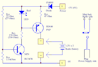
Ni-Cad Charger for Solar Cell Radio by BD140

A solar cell radio used a 3V (or two 1.2V) Ni-Cad battery in it. The battery can not be removed. It use a mini jack socket for charging. Its quiet difficult to find such a voltage charger. Here is the circuit to convert the voltage from the general power supply.

Temperature Controlled NICD Charger by IC LM311

This circuit is for a temperature controlled constant current battery charger. It works with NICD, NIMH, and other rechargeable cells. The circuit works on the principle that most rechargeable batteries show an increase in temperature when the cells becomes fully charged. Overcharging is one of the main causes of short cell life, hot cells pop their internal seals and vent out electrolyte. As cells dry out, they lose capacity.

Theory
The transformer, bridge rectifier, and 1000uF capacitor provide around 22 Volts of DC power to run the rest of the circuit. The 7812 regulator drops this to 12V to run the 311 comparator and 4011 nand gates.

The start switch is pressed to start the charging cycle. This causes the two 4011 nand gates, which are wired as an r-s flip-flop, to go into the charging mode. The Red LED is lit, and the VMOS FET current switch is turned on. Charging current runs though the battery pack. If the battery starts out warmer than the reference temperature, the circuit will not switch into charging mode. Let the pack cool down. When the battery pack reaches a full state of charge, the differential temperature sensor causes the flip-flop to switch off, turning off the VMOS current switch, and lighting the Green LED.

The 7805 voltage regulator is wired as a constant current regulator. This provides a safe maximum charge current for a number of different cell types. The 500 ohm resistor across the VMOS FET sets the trickle charge current which flows through the battery pack after the bulk charging is finished.

The 1N5818 diode prevents the pack from discharging if the AC power is turned off.

The resistor, diode, and capacitor around the start switch cause the circuit to auto-start when power is first applied.

The differential temperature sensor circuit works by presenting two voltages to the input of the 311 comparator. The comparator output switches on or off depending on which input is at a higher voltage than the other. As the thermistors warm up, their resistance drops, lowering the associated comparator input. Since there are two sensors, the room temperature can vary and the circuit will only react to the difference in temperature between the sensors.

Tuesday, May 13, 2008

Auto Charger battery 12V by IC 741


This circuit Auto Charger battery 12V will quickly and easily charge most any lead acid battery. When the battery is fully charged, the circuit Relay switches off and lights a LED.